
Manufacturing a smartphone, assembling automotive sensors, or servicing medical instrumentation all share a common vulnerability: the risk that an invisible electrostatic event will compromise reliability before the product ever reaches its end user. Voltage differentials too small to be felt by human touch routinely breach insulation barriers inside integrated circuits, weakening oxide layers and shortening service life. Understanding why a discharge below typical perception thresholds poses such a threat—and how structured countermeasures mitigate that threat—determines whether production yields meet targets or waste climbs unexpectedly.
What ESD is and how an invisible spark destroys components
Electrostatic discharge (ESD) occurs when accumulated charge transfers abruptly between two objects at different potentials. Even a sub‑50‑volt event can puncture the gate oxide of a MOSFET or degrade junction integrity in CMOS logic. The brief current pulse (nanoseconds) generates localized heating sufficient to melt semiconductor junctions or create micro-fractures that manifest as latent defects weeks later.
Picture yourself walking across a synthetic carpet on a dry winter day. Your body picks up electrons through friction, building a potential difference relative to grounded metal. The moment your fingertip approaches a door handle, a tiny arc neutralizes that imbalance. That everyday phenomenon scales down to the workshop floor, where an operator’s shoe sole rubbing polyester mats charges their body to several thousand volts. Any conductive path—direct contact, inductive coupling, or field effect—can channel that energy into a component lead.
Sensitivity thresholds vary by device architecture. According to the EOS/ESD Association’s 2026 Technology Roadmap, future semiconductor nodes are projected to fail at charge levels approaching 10 V, a figure that underscores the narrowing margin for error. Older bipolar transistors tolerated hundreds of volts; modern FinFET logic and gallium-nitride power devices can sustain permanent damage from pulses that a voltmeter would barely register.
The physical mechanism behind failure centers on dielectric breakdown. Gate oxides in MOSFETs measure only a few nanometers thick. When transient voltage exceeds the oxide’s breakdown strength, a conductive filament forms, permanently shorting gate to substrate. Alternatively, the discharge may inject sufficient energy to raise junction temperature beyond the silicon melting point, creating localized voids or alloying dopant profiles. Either outcome shifts electrical parameters—threshold voltage, leakage current, transconductance—away from specification.
Manufacturers quantify susceptibility using Human Body Model (HBM), Charged Device Model (CDM), and Machine Model (MM) test standards. HBM simulates a charged person touching a pin; CDM models the device itself acquiring charge and discharging through a single lead. A component rated HBM Class 1A withstands only a few hundred volts, while Class 3C tolerates several thousand volts. The trend, however, moves relentlessly toward lower withstand voltages as feature sizes shrink and supply voltages drop. Relying on robust packaging to protect sensitive die has become insufficient when next-generation optoelectronics and high-frequency RF amplifiers incorporate bare-die interconnects and direct-chip-attach assemblies.
Static control begins with recognizing that charge generation is inevitable wherever dissimilar materials separate. The triboelectric series ranks materials by their tendency to gain or lose electrons: rubbing polyethylene against steel transfers charge predictably. Large surface areas—conveyor belts, plastic trays, synthetic garments—amplify the effect. Once charge accumulates, it seeks the fastest path to ground. If that path includes a semiconductor junction, damage follows. Effective mitigation therefore requires both preventing charge buildup and providing controlled discharge routes that bypass vulnerable circuitry. For organizations assembling or testing electronic systems, implementing an ESD protection strategy anchored in validated equipment and procedural discipline transforms abstract risk into measurable outcomes. Without such measures, even a sub‑50‑volt event can compromise reliability.
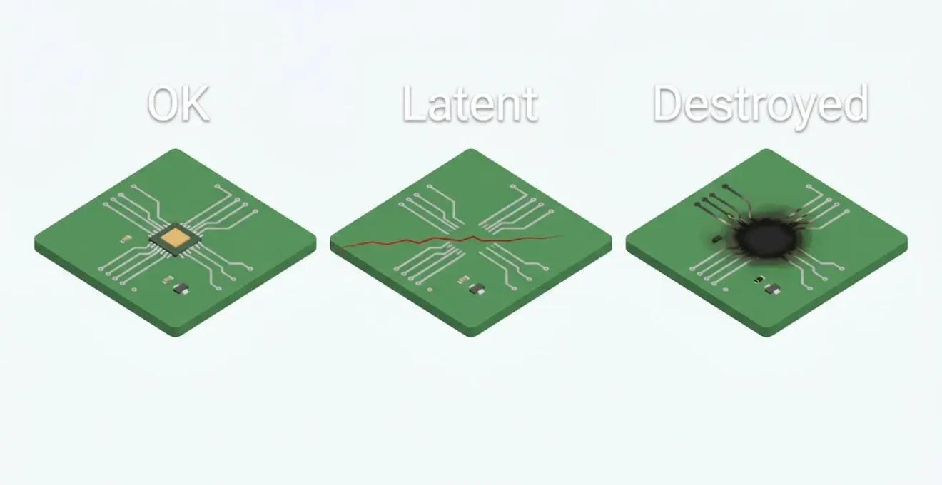
The three failure modes: latent, parametric, and catastrophic
Damage from electrostatic discharge does not always announce itself immediately. A circuit may leave the assembly line passing all functional tests, yet harbor microscopic defects that accelerate degradation in the field. The industry classifies ESD damage into three categories based on severity and observability: catastrophic, parametric, and latent.
Hidden cost of latent failures: Latent defects represent the most insidious consequence of inadequate static control. A component weakened by a sub-threshold discharge may operate within specification during production testing but fail prematurely under thermal cycling or voltage stress in service. Field returns attributed to « infant mortality » often trace back to undetected ESD events during manufacturing. Because the failure occurs months after assembly, root-cause analysis becomes difficult, and warranty costs accumulate without triggering immediate corrective action on the factory floor.
Catastrophic failure leaves no ambiguity. The discharge energy exceeds the component’s absolute maximum rating, creating an immediate short or open circuit. A gate oxide punctures completely, a bonding wire fuses, or a junction welds shut. Automatic test equipment flags the part as non-functional, and it never ships. While catastrophic failures inflate scrap rates and waste material, they at least surface during in-process inspection. The defect gets caught, the lot gets quarantined, and operators receive feedback linking process deviations to yield loss.
Parametric degradation sits between latent and catastrophic extremes. The component still functions, but key specifications drift. Leakage current climbs from nanoamperes to microamperes; propagation delay lengthens; noise margin shrinks. Parametric shifts may escape generic go/no-go testing if test limits carry generous margins, yet the part’s reliability has been compromised. In high-volume production, parametric outliers skew process-capability indices and trigger false alarms during statistical quality control, consuming engineering time without revealing the ESD root cause.
Consider a scenario encountered by a quality engineer at a mid-sized contract manufacturer assembling automotive radar modules. A new batch of RF amplifiers exhibited a 15 percent rejection rate during final RF performance testing—gain compression appeared earlier than datasheet specifications predicted. Initial suspicion centered on component lot variation or solder-reflow thermal profiles. Only after an abstract integrated circuits are susceptible to did the pattern become clear. Operators had been handling sensitive devices while accumulating body voltage, injecting sub-catastrophic pulses that weakened internal matching networks. Implementing a basic ESD kit—proper mats, continuous-coil wrist straps, and common-point grounding—alongside operator retraining reduced the rejection rate to 1 percent within a month. The financial impact: reclaiming approximately $18,000 per quarter in previously scrapped modules, against a one-time investment of roughly $3,200 for workstation upgrades.
Research into failure mechanisms confirms that latent defects often outnumber immediate catastrophic events. Micro-cracks in metallization, partial oxide thinning, and localized junction damage accumulate silently until thermal stress or electrical transients during normal operation push the weakened structure past its breaking point. Unlike catastrophic shorts that light up failure-analysis microscopes with obvious melt traces, latent damage requires cross-sectional transmission electron microscopy or time-dependent dielectric breakdown (TDDB) testing to detect. By the time a latent defect manifests as a field failure, tracing it back to a specific handling lapse weeks or months earlier proves nearly impossible.
The pillars of an ESD-safe environment: equipment, standards, and best practices
Controlling electrostatic discharge demands more than purchasing a wrist strap and hoping for compliance. A robust program integrates conductive or dissipative materials, continuous monitoring, operator training, and adherence to industry standards. The concept of an ESD Protected Area (EPA) formalizes this integration: a designated zone where all surfaces, tools, personnel, and packaging maintain controlled resistivity and common electrical potential.
10V
Projected ESD failure threshold for next-generation semiconductor nodes by 2030
The foundation layer of an EPA starts with flooring and work surfaces. Conductive or dissipative mats cover benches and floors, providing a defined path for electrical charges to safely dissipate. In ESD-protected areas (EPA), these factory-installed surfaces typically have a surface resistivity between 10⁶ and 10⁹ ohms per square—low enough to drain static electricity within seconds, yet high enough to prevent hazardous current flow in the event of contact with a live circuit. Mats connect to facility ground via a common-point ground system, ensuring all surfaces share the same reference potential. Neglecting this grounding step transforms an ESD mat into an insulator: charge drains from the component onto the mat, but without a ground path, the mat itself becomes charged.
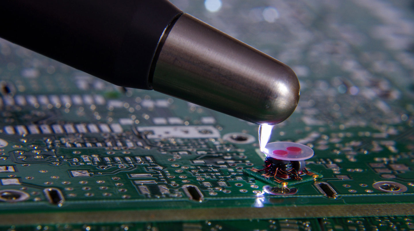
Personal grounding comes next. Wrist straps and heel grounders bond operators to the EPA ground network. A wrist strap consists of a conductive band, an adjustable elastic strap, and a coiled cord terminating at a banana plug or snap connector. Inline resistors (typically 1 MΩ) limit fault current while allowing static to dissipate. Continuous monitors test strap integrity in real time; if the circuit opens—broken wire, loose clasp—an audible alarm halts production. Heel grounders, worn inside conductive shoes or clipped onto shoe soles, suit environments where mobility or dual-hand work makes wrist straps impractical. Both methods rely on discipline: a strap lying on the bench provides zero protection.
Air ionization addresses insulators that cannot be grounded. Plastics, glass, and many production fixtures generate charge through friction yet remain electrically isolated. Ionizers emit balanced streams of positive and negative ions that neutralize surface charge without physical contact. Overhead ionizing blowers cover large areas; benchtop units target specific workstations; ionizing air nozzles clean charged dust from optical assemblies. Regular calibration verifies that ion output remains balanced and discharge times stay within specification—unbalanced ionization can worsen the problem by preferentially charging objects to one polarity.
Beyond hardware, procedural controls and documentation close the loop. Standard operating procedures define ESD handling protocols: when to don wrist straps, how to transport sensitive devices, which packaging materials are approved. Periodic audits verify compliance—checking mat resistivity monthly, testing wrist-strap continuity daily, and inspecting garment conductivity quarterly. Training programs educate operators on charge generation mechanisms and the business impact of ESD damage, transforming rote compliance into informed participation. Successful programs also track metrics: defect rates correlated with EPA audit scores, cost of scrap attributed to ESD versus cost of prevention infrastructure, and traceability linking field returns to specific manufacturing lots.
Material selection extends EPA principles to packaging and transport. Conductive or dissipative bags, trays, and foam cushion components during storage and shipment. Shielding bags—metallized films enclosing dissipative inner layers—protect against both electrostatic discharge and electromagnetic interference. Marking packaging with ESD-sensitivity symbols alerts handlers downstream, reducing the likelihood that a protected component gets carelessly tossed onto a charged surface during unpacking.
- Dissipative work-surface mat with verified surface resistivity (10⁶–10⁹ Ω/sq) bonded to common-point ground
- Continuous wrist-strap monitor providing real-time operator-grounding verification
- Balanced ionization system with calibration records confirming fast discharge neutralization
- ESD-safe storage bins and packaging materials (conductive or dissipative) for component staging
- Documented audit schedule covering mat resistance, strap continuity, garment conductivity, and ionizer balance
What you need to remember to take action
Electrostatic discharge does not announce itself with sparks or smoke until the damage is done. By the time a component fails on the test bench or in the field, the root cause—a momentary voltage spike weeks earlier—has vanished. Preventing ESD-related losses therefore hinges on embedding protective infrastructure and disciplined procedures before defects arise, rather than reacting to scrap reports after the fact.
The business case for ESD control rests on straightforward arithmetic. Scrap costs accumulate visibly: rejected modules, rework labor, delayed shipments, and warranty claims. Investment in ESD protection—grounded mats, monitored wrist straps, ionizers, and operator training—represents a one-time or periodic expense that scales predictably with workstation count. Field data consistently demonstrate that facilities maintaining rigorous EPA protocols report defect rates well below one percent, while sites with ad hoc static control struggle with rejection rates in the mid-teens. When a single scrapped RF amplifier costs $120 and a fully equipped workstation requires a $3,200 outlay, breaking even demands preventing fewer than 27 rejects—a threshold most disciplined programs achieve within the first production quarter.
- Verify mat surface resistivity falls within 10⁶–10⁹ Ω/sq using a calibrated meter
- Confirm wrist-strap ground cord connects securely to common-point ground terminal
- Test wrist-strap continuity through skin contact at shift start using inline tester
- Check ionizer balance monthly; adjust emitter polarity if ion imbalance exceeds ±10 V
- Remove insulating materials (uncertified plastics, paper, glass) from the immediate work zone
- Store sensitive components exclusively in shielding bags or conductive foam until use
- Document audit results and corrective actions in a retrievable log for traceability
Standards provide the roadmap. IEC 61340-5-1 outlines requirements for establishing and maintaining an ESD control program, specifying resistivity limits, grounding methods, and qualification procedures. ANSI/ESD S20.20 offers a parallel framework widely adopted in North America. Both standards emphasize a systems approach: isolated interventions—buying one wrist strap, placing one mat—deliver marginal benefit unless integrated into a comprehensive program covering personnel, workstations, packaging, and continuous improvement. Certification to these standards signals to customers and auditors that static control has moved from anecdotal practice to verifiable process discipline.
Ultimately, protecting electronics from electrostatic discharge requires shifting perspective. Static electricity is not an occasional nuisance; it is a continuous background threat whose consequences compound over production volume. Waiting for scrap rates to climb before investigating ESD damage guarantees that months of defective product have already shipped or filled rework queues. Forward-looking organizations treat EPA infrastructure as manufacturing table stakes—equivalent to calibrated test equipment or climate-controlled assembly areas—and measure success not by detecting ESD damage but by preventing it in the first place. When invisible sparks no longer dictate yield curves, engineering effort redirects toward innovation rather than firefighting, and reliability metrics reflect design intent rather than handling lapses.